 32 nm process
Common
Rarity: Common
The most frequent rarity: most Wikipedia articles become Commons.
Rarity follows how well known the article is: its views on the French and English Wikipedia over a year, and the number of languages it exists in.
At a glance
- Class
- Notion
- Domain
- Science and technology
- In collections
- Nobody has pulled it yet.
What Wikipedia says
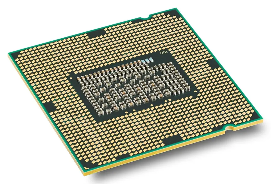
The 32 nm node is the step following the 45 nm process in CMOS (MOSFET) semiconductor device fabrication. "32-nanometre" refers to the average half-pitch (i.e., half the distance between identical features) of a memory cell at this technology level.
Excerpt from the Wikipedia article “32 nm process”, under the CC BY-SA 4.0 license. Read the article on Wikipedia
Image: Eric Gaba (Sting - fr:Sting), CC BY-SA 3.0, via Wikimedia Commons.
Open free boosters and add 32 nm process to your collection.
Play for free