
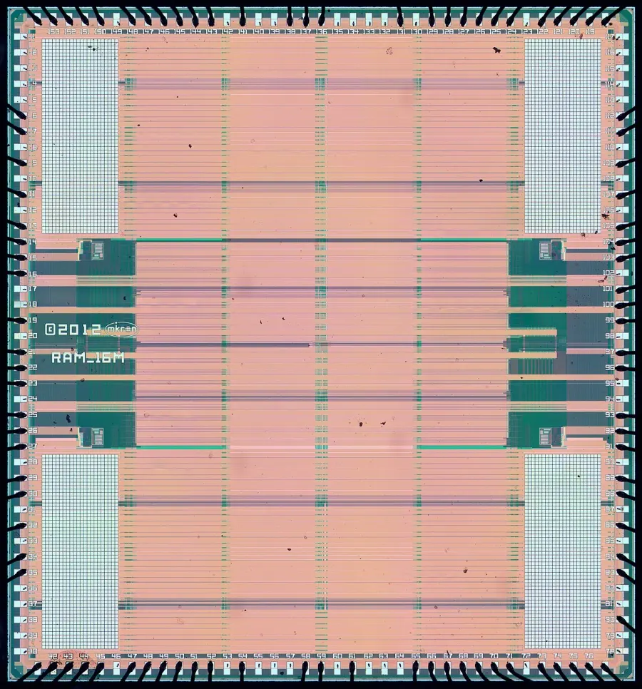
 90 nm process
Common
Rarity: Common
The most frequent rarity: most Wikipedia articles become Commons.
Rarity follows how well known the article is: its views on the French and English Wikipedia over a year, and the number of languages it exists in.
At a glance
- Class
- Notion
- Domain
- Science and technology
- In collections
- Nobody has pulled it yet.
What Wikipedia says
The 90 nm process refers to the technology used in semiconductor manufacturing to create integrated circuits with a minimum feature size of 90 nanometers. It was an advancement over the previous 130 nm process. Eventually, it was succeeded by smaller process nodes, such as the 65 nm, 45 nm, and 32 nm processes.
Excerpt from the Wikipedia article “90 nm process”, under the CC BY-SA 4.0 license. Read the article on Wikipedia
Image: ZeptoBars, CC BY 3.0, via Wikimedia Commons.
Open free boosters and add 90 nm process to your collection.
Play for free